Contact information:
Facility Manager: Dr. Yi Hu
Location: Sem Sælands vei 24
0371 OSLO
Norway
Instruments:
- SFA 2000 from Surforce LLC
- CellTIRF-Line system from Olympus
- Home-built OpenSPIM with great flexibility and adaptability to fit for different experimental purposes
- Photolithography processing
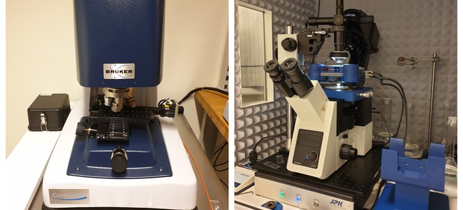
- NanoWizard 4 AFM from JPK
- ContourGT 3D Optical Microscopy
Description of services:
- NanoWizard 4 AFM from JPK
- Surface force measurement with in-situ fabricated calcite probe
- Surface characterization of granite after experimental slip surface
- Quantitative characterization of dry samples
- Mapping of material properties
- Characterization of electrical, electromechanical or magnetic sample properties
- Hands-on Training for using AFM
- ContourGT 3D Optical Microscopy
- 3D surface measurement of materials
- Hands-on Training for using ContourGT
- OpenSPIM
- Photolithography Processing
- Hands-on Training for fabricating microfluidic channels
- Help design microfluidic channels with different sizes, from nm to cm
Imaging and Photolithography in Flow Lab
Atomic force microscopy (AFM) which is one type of scanning probe microscopy (SPM) has three major abilities: force measurement, imaging, and manipulation. In force measurement, AFM can be used to measure the forces between the probe and the sample. One of our researchers used it to measure the interfacial forces between two calcite surfaces in CaCO3-saturated solutions. [1] The force reaction between the probe and the sample can be used to form three-dimensional shape images at a high resolution. This can be achieved by recording the height of probe which corresponds to the constant probe-sample interaction. The forces between tip and sample can be used to change the properties of the sample based on user’s manipulation. ContourGT 3D Optical Microscopy provides high performance of non-contact 3D surface structure measurements ranging from nanometers to centimeters. It can be used to measure surface profile, roughness, step height, microstructure, and other surface parameters. One of our researchers used it to observe the topography of the calcite–water interface. [2] The SPIM technology promises to revolutionize several fields of biological research by offering fast and optically-sectioning 3D acquisition of fluorescing specimen over time. Photolithography is a process used in microfabrication to pattern parts of a thin film. Our researchers has consistently fabricated different types of microchannel and applied them into their experiments. The laboratory can by appointment be used in research activities or/and assisting students at the Department of Physics.
- Adhesive forces between two cleaved calcite surfaces in NaCl solutions
- Xurography for microfluidics on a reactive solid