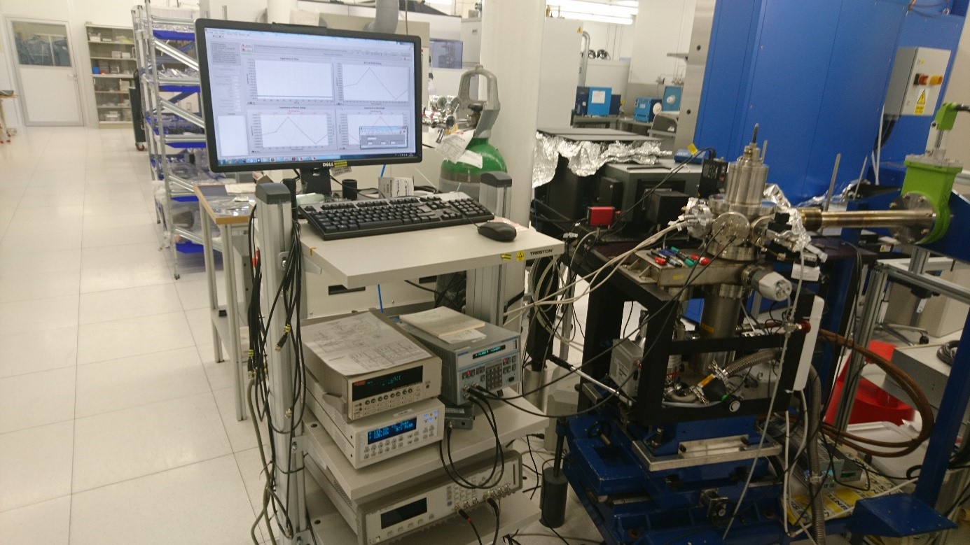
Online-setup for opto-electronic characterization at MiNaLab
During the crystallization of Si melt, the structure and impurity incorporation are strongly affected by vacancy and interstitial defects. At temperatures around and above 1000oC, the concentration of these defects is high, while at room temperature the concentration is below the detection limit of most of characterization methods. In order to be able to study vacancies and interstitials, we can artificially increase their concentration by particle irradiation.
The Online-setup at MiNaLab enables users to perform optical and electrical characterization right at the beam line (on-line) of a MeV ion implanter (see Fig. 1). The samples can be kept at temperatures between 30 K and 320 K during irradiation/implantation using a closed-cycle He cryostat.
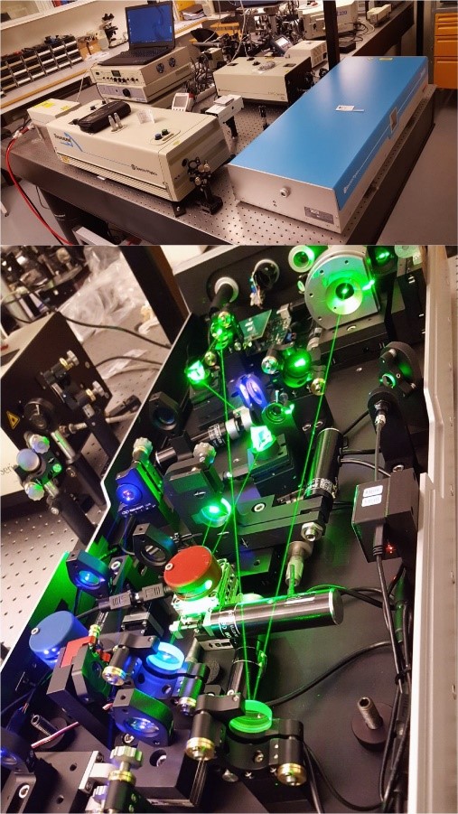
Photoluminescence laboratory at MiNaLab
The photoluminescence laboratory includes time-integrated, time-resolved and imaging photoluminescence spectroscopy setups using several fixed-wavelength lasers. Recent upgrade with ultrafast tunable laser source transformed the system to the state of the art level expanding the analytical capabilities by additional methods of photoluminescence excitation (PLE) and ultrafast pump-probe absorption spectroscopy, as well as facilitating methods relying on multi-photon/non-linear interaction. The optical characterization facility is a critical component of both fundamental and applied research providing essential feedback for the material synthesis and device processing. It is extensively used within a number of projects on solar energy conversion, and also acts as an important educational tool.