The aim of this project is to design, to fabricate and to characterise radiation detector using silicon carbide (SiC), primarily for dosimetry applications. Through this project, the student will learn the complete sensor fabrication cycle from design, fabrication to qualification. In this cycle, the student will be trained and to use important work tools such as TCAD simulation, fabrication and charactersiation techniques.
Dosimetry is used in many fields within radiation protection. Quality Assurance (QA) in particle therapy is the key application focus in this project. Novel radiation therapy in cancer treatment have unique radiation properties that continuosly brings demands in modern therapy QA. Solid-state detectors especially those that are silicon-based are reliable, and can be manufactured using matured, well-established technology. They provide many advantages, for example: easy coupling with readout electronics, fast response time, and provision of a real-time online monitoring system. By replacing silicon with SiC, one can further improve detector properties. For example, higher tissue equivalence that can provide an improved estimation of radiobiological effectivenss (RBE) of the received dose in patients. SiC as a material alone, also allows for other advantages such as higher breakdown voltage and radiation tolerance. SiC technology is today gradually becoming a matured technology in power electronics. For radiation detection, more studies are required to use them as advanced radition detectors and dosimeters. In this project, one will study the suitability of using SiC as radiation detectors through TCAD (Technology Computer Aided Design), fabrication and experimental characterisation. The entire team at SINTEF and at UiO will work closely with application scientists and collaborators to understand the specification requirements for therapy QA.
The project will be carried out by the student through the following tasks:
- TCAD Simulation – Process Simulation
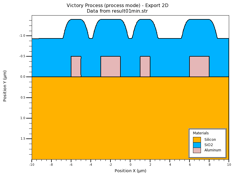
The Student will carry out TCAD simulation (either Silvaco or Synopsys Sentaurus) to understand the fabrication of silicon carbide detectors, both Schottky diode and P-N junction diode. The obtained doping profiles and device structure will then be investigated using device simulation.
- TCAD Simulation – Device Simulation
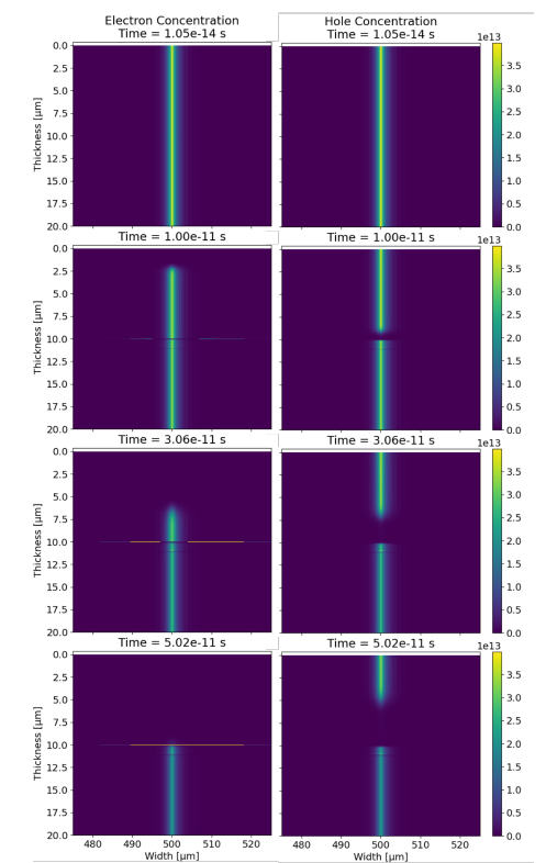
Based on the simulated doping profiles and structures, the device properties will be simulated using initial design parameters.The simulated electrical properties such as I-V and C-V characteristics will determine the most optimal sensor design. The student will work closely with the supervisors from the initial design phase, and several design and simulation iterations are expected. The electrical measurements from task 3, when completed can also used to refine the simulation model.
Kjetil Gulli, "Simulation of Schottky Diode-Based Silicon Carbide Radiation Detectors", duo.uio.no/handle/10852/95438
- Sensor fabrication
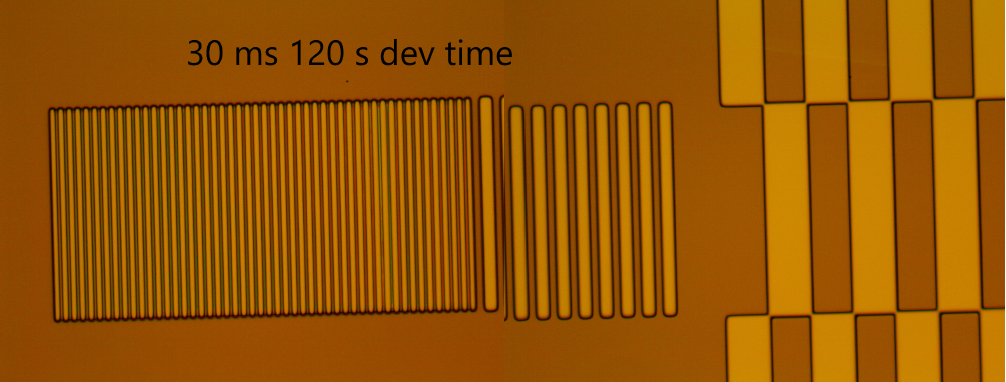
Using the simulation results, a technology plan will be drawn.The student will fabricate SiC detectors at the cleanroom facilities at the LENS group. The foreseen processes involved will be lithography (see pictures below), e-beam evaporation of metal for electrode contacts, high temperature furnaces and ion implantation. The student will also learn the complete fabrication technology process, the importance of processes and procedures such as sample cleaning.During the fabrication phase, it will also be optional for the student to perform and to learn other characterisation techniques such as thin film ellipsometry and 4-point probe measurement.
- Electrical characterisation
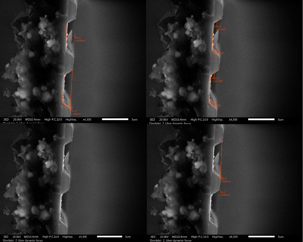
The fabricated sensors must then be characterised using a manual probe station.I-V (Current- Voltage) measurement and C-V (Capacitance-Voltage) measurement will first be carried out. For more advanced detector design, such as those with multiple active elements, inter-element resistance will also be measured.The results will then be compared with the simulation from task 1.
- Full evaluation
A full evaluation of the simulation and final electrical results will be carried that will verify the optimal design. The evaluation will provide a new, improved design for future SiC detector generations.
Additional tasks (Optional)
If time allows and are of interests for the student, the following additional tasks can be carried out:
- Material and defect studies
The function of a SiC detector is affected by their intrinsic properties.Detailed studies using optical spectroscopy and Deep Level Transient Spectroscopy (DLTS) will provide a thorough understanding on SiC.
- Signal generation simulation
Charge injection that emulates the incident radiation in the proposed radiation detector can be simulated. The generated signal will then simulated. This simulation can further enhance the understanding of the sensor in terms of the sensor design and functionalities.
- Radiation measurements
Once the sensors are electrically characterised, they must then be characterised using radioactive sources or at radiation beamlines. These can be carried out in agreement with our collaborators such as are the European Synchrotron Radiation Facilities, Oslo Cyclotron and Czech Technical University in Prague.